| Date: | February 16 |
| Lecture: | 13 |
| Handout | hand13.docx |
| Status: | Complete |
| Code | lec13_dp.vhdl lec13_tb.vhdl lec13.wcfg |
| Lesson Slides | CSCE_436_Lec13.pptx |
7 Series (Artix 7) Library
The Artix 7 FPGA has a lot more than just logic gates and flip flops. There are a lot of special resources built into the chip. Access these resources requires knowing what these resources are and how to instantiate them in a design. Today we will talk about both.To start your journey, you need to look through the first page of the 7 Series FPGA Family Overview. The third page lists quantities how many of these resources our Artix 7 chip on our Nexys Video boards have. For reference we are using the XC7A200T chip and the SBG484 package. It has some pretty impressive stats. Of significance to us is the block rams and the DSP blocks.
In our upcoming Lab2, you will need a large RAM to store 18-bit audio samples streaming in from the Nexys Video board. The Xilinx FPGA on our board, a Artix 7, contains built in block RAMs (BRAMs). You can select of the three main BRAMS configuration (BRAM_SDP_MACRO, BRAM_SINGLE_MACRO, BRAM_TDP_MACRO) available in the UNIMACRO library. We will be using a BRAM_SDP_MACRO in our design. According to Vivado Design Suite 7 Series FPGA Libraries Guide.
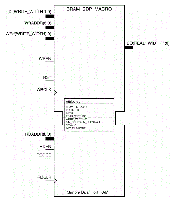
An example instantiation of the BRAM is given in the code block below. Note all the configuration is done in the generic section, while the port section takes care of the actual wiring of the BRAM into your design. Remember that this call is actually mapping directly onto a pre-defined BRAM inside the Artix 7 chip.
    ----------------------------------------------------------------------------
    -- Reference:	Vivado Design Suite 7 Series FPGA Libraries Guide
    --              UG953 (v 2012.4) July 25, 2012
    --
    -- Page:	10
    -----------------------------------------------------------------------------
    sampleMemory: BRAM_SDP_MACRO
	generic map (
		BRAM_SIZE => "18Kb", 			-- Target BRAM, "18Kb" or "36Kb"
		DEVICE => "7SERIES", 			-- Target device: "VIRTEX5", "VIRTEX6", "SPARTAN6, 7SERIES"
		DO_REG => 0, 					-- Optional output register disabled
		INIT => X"000000000000000000",	-- Initial values on output port
		INIT_FILE => "NONE",			-- Not sure how to initialize the RAM from a file
		WRITE_WIDTH => 18, 				-- Valid values are 1-72 (37-72 only valid when BRAM_SIZE="36Kb")
		READ_WIDTH => 18, 				-- Valid values are 1-72 (37-72 only valid when BRAM_SIZE="36Kb")
		SIM_COLLISION_CHECK => "NONE", 			-- Collision check enable "ALL", "WARNING_ONLY", "GENERATE_X_ONLY" or "NONE"
		SRVAL => X"000000000000000000")	-- Set/Reset value for port output
	port map (
		DO => readOutput,				-- Output read data port, width defined by READ_WIDTH parameter
		RDADDR => vecAddrRead,			-- Input address, width defined by port depth
		RDCLK => clk,	 				-- 1-bit input clock
		RST => reset,					-- active high reset
		RDEN => cw(5),					-- read enable
		REGCE => '1',					-- 1-bit input read output register enable - ignored
		DI => writeInput,				-- Input data port, width defined by WRITE_WIDTH parameter
		WE => cw(3 downto 2),			-- since RAM is byte read, this determines high or low byte
		WRADDR => vecAddrWrite,			-- Input write address, width defined by write port depth
		WRCLK => clk,		 			-- 1-bit input write clock
		WREN => cw(4));					-- 1-bit input write port enable
Now an activity for the class. Determine what will happen inside the RAM
defined above when subject to the following signals.
    -- vecAddrRead = vecAddrWrite - 1
    -- writeInput <= "10101010101010" & vecAddrWrite(3 downto 0);
    cw(5) <= '1', '0' after 7 us, '1' after 8 us;	-- READ ENABLE
    cw(4) <= '1', '0' after 3 us, '1' after 4 us;	-- WRITE ENABLE
    cw(3 downto 2) <= "11", "10" after 4 us, "01" after 5 us, "11" after 6us; -- BYTE WRITE ENABLE
    cw(1 downto 0) <= "01";				-- COUNTER CONTROL
Packages
Packages are a nice way to hide lots of component declarations that go between the architecture statement and the BEGIN statement. One of the main contributors of complexity in software is redundancy. In this scenario, having an entities declaration in several different architectures is redundant. Pulling all these declarations into one file would eliminate this redundancy and make the code much easier to maintain and update. So how do you create a Package? Here is a package that I created for lab2. Then anytime you want to use this package, just include the following at the top of your file.use work.lab2Parts.all; -- all my components are declared here
2-Line Handshake
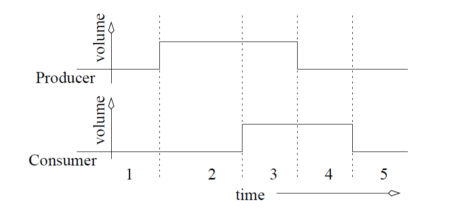
In most cases, digital systems require data from the external world in order to perform their tasks. In cases where the digital system and the outside word operate on independent clocks, the transfer of data is complicated by the lack of a common clock. To understand how a reliable transfer of data can be performed in this circumstance, consider the following scenario of a producer trying to deliver a packet of candies to a consumer.Two participants associate in the scenario called producer and consumer. The producer has a bag of 32 candies; (the number of candies in the bag really does not matter). The candies are to be given to the consumer and the producer is to receive an acknowledgment from the consumer of their receipt. Unfortunately, the producer is blind-folded and is wearing a rather thick pair of ski mittens so they do not know when the consumer has actually taken the candies. The producer and consumer must synchronize the transfer of candies using signals sent with their voices. The transfer protocol is described in the following four steps:
- The producer stumbles into consumer's room and calls out, "Candies, Candies, . . ." (non-stop).
- The consumer gets up, takes the box of candies and then calls out, "Received, Received, . . ." (non-stop).
- The producer upon hearing the consumer has received the candies stops calling "Candies" and walks out of the room.
- The consumer upon hearing the producer has stopped calling out "Candies," stops calling out "Received."
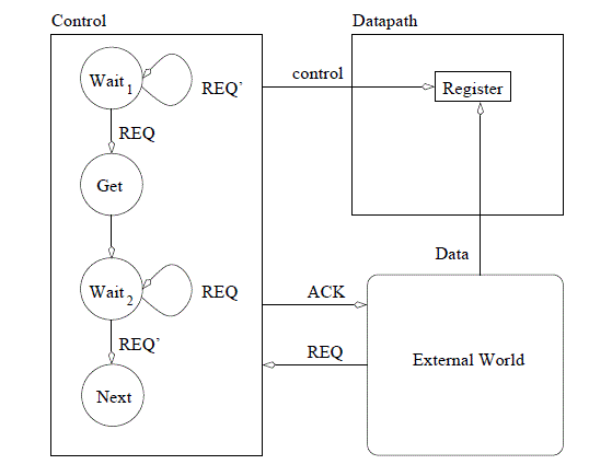
1. while(REQ==0); // Do nothing but wait
2. register = DATA // Latch the data
3. ACK=1; // Acknowledge the producer
4. while(REQ==1); // Do nothing but wait
5. ACK=0; // Acknowledge the producer
In Line 1 and Line 4, the body of the while loops are empty; there is nothing to do but wait. Furthermore, with respect to the external world, the ACK and REQ signals act as status and command bits, respectively. The algorithm above is translated into datapath and control in Figure 13.3.
Datapath and Control Exercise
1. while(1) {
2.     while(REQ == 0);
3.     KEY = data;
4.     ACK = 1;
5.     while(REQ == 1);
6.     ACK = 0;
7.     match = 0;
8.     for(i=0; i<2048; i++) {
9.         MBR = RAM[i];
10.        if (MBR == KEY) {
11.            match=match+1;
12.        } // end if
13.    } // end for
14. } // end while