Homework #6
Guidelines
- Complete your work on green engineering paper
- Staple in upper left if more than one sheet.
- Format the top of the first sheet as follows.
| ECE 383 | [Your name] | HW#9 | [Due Date] | [Page ref]
|
The page reference for the first page of a four page document would be 1/4, the
second page of this document would be labeled 2/4 and so on.
- Do not write on the back side of the green engineering paper
- Digital copies of all code, testbenches, and waveforms will also be submitted via BitBucket.
- Crusty the engineer is a well intentioned employee in your organization
who, unfortunately, is caught in some kind of 70's time warp. Crusty is
convinced that a FSM built using discrete logic gates will outperform your
shiny new 100Mhz FPGA design. Arguing with Crusty has come to nothing and its
time to put an end to this once and for all. You are going to do the
calculations to see how fast a discrete logic gate realization can run.
You are to build the FSM using the the architecture given in Lecture 9.
Use the positive edge triggered
flip flops inside the SN74LS273N chip, and the AND, OR and NOT gates inside
the SN74LS08N, SN74LS32N, and SN74LS04N chips respectively. You are to
assume that the logic inside the MIE and OE boxes are 2-level combinational
logic (solved using a kmap). You will need to pull the technical documents
for the chips by searching Digi-Key and clicking on the Datasheet in
the part view. When given a choice, always use the worst-case time estimates
from the data sheets.
To make your point you will need to show Crusty the details of your calculations,
making sure to document where the numbers came from.
- Calculate the minimum clock period and the maximum clocking frequency.
- How many times faster is the discrete logic realization compared
to a 100Mhz FPGA realization?
- Check out the Logic Families
entry on wikipedia. Excluding the G series, what TTL family type should have the
highest clocking rate?
- Provide a rough estimate of the clocking frequency of a FSM built from this
type of logic. Making sure to show your calculation.
- List at least two other performance related dimension could you
argue that an FPGA solution would be superior. Briefly describe
how you would make your case.
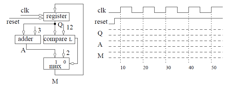
-
Complete the timing diagram below assuming that the register is
positive edge trigger and has an asynchronous active low reset.