Building
a Pipelined RISC Processor
----CSCE 430/830 Term Project, Fall 2008
1. Introduction
This document is prepared for the CSE 430/830 term project��building a pipelined RISC processor. The goal of this project is to familiarize students with the design and implementation of a pipelined RISC processor. Students will be building a processor from ground-up to implement some simple functions. In addition, students need to write an assembler that detects hazards and optimizes the MIPS code to minimize stalls. This is a group project where each group can have three to five members. The project presentation will be held during the dead week.
2. Project Description
In this project, you will be building a pipelined RISC microprocessor to support computing in embedded systems. Your design must be conducted on Altera��s Quartus II software. You can use graphical gate-level design tool or high-level language such as VHDL. Both methods are supported in the software. The processor does not need to support floating point calculation.
Your first task is to come up with a basic design. You will need to decide on the number of registers available, the sizes of data bus and instruction bus, and the amounts of data and instruction memories needed. Remember, a more complicated design often results in more power consumption. However, not sufficient design (e.g. not enough registers) can also result in higher power consumption due to more frequent memory accesses. Once you have the basic structure of your processor, you then need to design the instruction format and instruction set. You should include only the instructions that are necessary. The most commonly used should also be optimized for the best performance (Amdahl��s law). If you want to include an exotic instruction or operation, you must be able to justify the need for it since more hardware will be used. For this semester, you are required to either build a vending machine controller or implement matrix multiplication. The processor will be used to accept inputs and produce outputs accordingly. More details about the software component can be seen in the next section. Don��t be surprised if you need to revise or redesign your instruction set as your idea becomes more mature.
The major components to be developed in this project include program counter (PC), register files, decoder, ALU, instruction memory (IM) and data memory (DM), as well as some supplementary parts such as clock, forwarding unit, pipeline registers, I/O, and etc. Some of the components (PC, IM, and DM) will not change too much during the course of your design, and they should be constructed as early as possible. To simplify the project reasonably and assist your design, we will provide workable reference designs for some of the components, including clock, IM, DM, and I/O. You can also start building basic components such as one bit ALU and most significant bit ALU. Once you have decided on the size of data, you can use these ALUs to construct the final ALU. You also need to create a forwarding unit that can minimize stalls by resolving data hazards. To build a pipelined processor finally, it could be a good idea to firstly build a non-pipelined processor that passes simulations and tests. After that, you can add the pipeline registers to pipeline your processor.
You will use MIPS assembly language (with your own instruction set) to write your application program for the software component. To convert the assembly program into a format that is readily for the memory in your design, you will need to write your own two-pass assembler. The assembler can be written in any language, such as Java, C, C++, Perl. In the first pass, your assembler resolves all the symbols. In the second pass, it needs to convert the instructions to the proper memory format. Your assembler also needs to detect other hazards (the data hazards are handled by the forwarding unit) and insert stalls as needed. Altera specifies the format, Memory Initialization Format (MIF) that your assembler must be able to generate. An MIF file example is provided in appendix A. Your assembler will take a text file containing your assembly instructions as the input and produce MIF files as the output. Possibly, there should be two files generated: 1) the instruction file that can be loaded into Instruction Memory (IM); 2) the data file that can be loaded into the Data Memory (DM). Your CPU will fetch instructions from the IM and execute them. You should start the basic implementation of your assembler as early as possible.
You also need to build a web-site for your progress report. This site must be informative and easy to navigate because it is going to be your project presentation and the final report. The information that should be in your web-site includes:
�� team name, team members and their duties (you��d better elect a team leader)
�� meeting log in substantial details (should be more than ��we met today and discussed for two hours.��)
�� the design of each component with necessary explanations
�� the design of your assembler, and how to use it
�� stumbling blocks and how you try to solve them
�� the performance of your CPU (e.g. clock speed, gate count)
�� special features (may entitle you for some extra-credits)
�� the final result (e.g. finish, not finish��what has not been completed)
If you can think of other useful topics not mentioned here, feel free to include them in your web-site.
The first thing to do for the project: form a team, think of a team name, and then start by learning some background, or working on simple components right away.
3. Software Component
For this part, you will write an assembly program based on your instruction set to implement specific application functionalities. You can either build a vending machine controller or implement matrix multiplication. Your system should adhere to the guidelines in the following. This will allow the grading to be much easier.
A) Vending machine controller
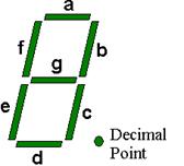
The vending machine delivers a package of gum which costs 55 cents. Due to the cheap price, this machine is only for use by students in this class with an 8-bit security code (for example, 11110000). We will set the security code on an 8-bit dip switch, simulate the user coin inputs by pressing the push buttons, and use the 7-sigment displays to show the system status. The following picture shows the 7-segment display for your output. You will have two such displays on the Altera UP2 experimental board. The system functionality is described as follows (a simple state transition diagram of the vending machine controller is provided in the following picture for your reference.).
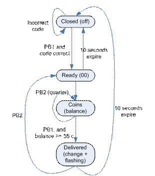
1. System closed: Initially, the system is closed, and the two displays (FLEX_DIGIT) are off.
2. System ready:
a) You set the security code on the FLEX_SWITH (8-bit dip switch) and press the left push button (FLEX_PB1) to open the service. If the security code is correct, the system enters a ��Ready�� state and the two displays will show 00. If the security code is incorrect, the system remains in initial state (displays are off).
b) At the ready state, the system expects your coins input within 10 seconds. If there are no coin inputs for 10 seconds, the system returns to the initial state, and the displays go off.
3. Coins input:
a) You insert coins by pressing the right push button FLEX_PB2. Every pressing simulates a quarter. As the coins are inputted, the displays will show the total amount of current balance. For example, if you put two quarters (press FLEX_PB2 twice), the display will show 50. Notice that this machine can not accept more than 75 cents. So if you input four quarters, you will get a balance of 00 unfortunately, i.e., the balance = sum mod 100 cents.
b) When all your coins are inputted, you hit the left push button (FLEX_PB1) to select the gum. If the current balance is not enough for the gum, the machine does nothing, waiting for more coins to be inputted.
4.
Gum delivery:
a) If the coins are enough for the gum, the system delivers the gum, and the decimal point of the right digit will begin flashing, indicating the gum is being released down the chute. At the same time, the displays will show the amount of changes.
b) At this time, the system expects you take the gum and changes within 10 seconds by hitting the right push button (FLEX_PB2).
c) If FLEX_PB2 is pressed, the system will return to its ��Ready�� state (waiting 10 second for next session, and if no more session, system closes and displays go off).
d) If FLEX_PB2 is not pressed, the system would resume initial closed state automatically (displays off), taking all the changes greedily.
B) Matrix multiplication
The second option requires you to implement matrix multiplication. Given two matrix A and B,

the product of A and B is C. Then,

To start the system, you are required to set the security code on an 8-bit dip switch. To facilitate the grading process, please use the matrix A and B provided above. The system functionality is described as follows:
1. System closed: Initially, the system is closed, and the two displays (FLEX_DIGIT) are off.
2. System ready:
a) You set the security code on the FLEX_SWITH (8-bit dip switch) and press the left push button (FLEX_PB1) to open the service. If the security code is correct, the system enters a ��Ready�� state and the two displays will show 00. If the security code is incorrect, the system remains in initial state (displays are off).
b) At the ready state, if there is no button pressed for 10 seconds, the system returns to the initial state, and the displays go off.
3. Matrix multiplication:
a) By pressing the right push button (FLEX_PB2), you system begin to calculate the product of matrix A and B. The result of the product is required to be saved in an array P stored row by row. For example, in the example given above,
P={1, 2, 3, -1, -2, -3, 0 -1, -2}
When the calculation is done, please show the first item in P, that is 1.
b) When the right push button (FLEX_PB2) is pressed, the next element in the array is displayed. If the current element is the last item in the array and the right push button (FLEX_PB2) is pressed, please show the first item in the array.
c) When the left push button (FLEX_PB1) is pressed, the previous immediate element in the array is displayed. If the current element is the first item in the array and the left push button (FLEX_PB2) is pressed, please show the last item in the array.
d) If there is no button pressed for 10 seconds, the system returns to the initial state, and the displays go off.
You can select either one of the two applications. (You do not need to do both.) In addition to the requirements specified in A) and B), you also need to set the security code on the DIP switches and output digits on the display. The security code is typically stored in the data memory[1]. A possible shortcut to output digits is to save the number representation of 0 through 9 in the data memory address from 0 to 9 beforehand, and simply fetch the number when you need to output a digit. For example, to output digit ��0�� on the display, you may store its representation (Probably, 11000000B to burn segment a,b,c,d,e and f, since the display is LOW-ACTIVE.) at memory address 0. Of course, this is only an option, and you can find other ways to do the digits output.
You will use memory-mapped I/O for input (from dipswitches and push buttons) and output (to displays). This is one of the most frequently asked questions. You will use this technique to access the input and output components on the board. Typically, we do not have special I/O instructions dedicated for reading inputs and writing outputs. Instead, we access I/O interface by using the load and store instructions with special addresses. In other words, some specific data memory addresses are interpreted not as accesses to the memory, but accesses to the I/O devices. For example, suppose we have an address space with 10 bits, which gives an address space from 0 to 1023. We can use the address 1022 for input and 1023 for output. In order to do I/O access, your system must recognize these addresses in the instruction, and issue appropriate control signals, so that the CPU reads data from input device and writes data to output device instead of memory. You may use multiple dedicated addresses if you have more I/O devices. The above only gives you a rough idea on this skill, and some more study may be necessary if you are not familiar with it.
4. Important Milestones
Even though this is a semester-long project, I would like to set a few milestones to prevent some of you from falling behind. The following assignments must be done by the due date. Otherwise, penalty may apply to your final grade. Here are the important dates.
��
group formed (send an email with a listing of
all members, your team��s name and the project web-site address to the TA). �C
September 8, 2008
��
basic design finished, including instruction
length, instruction set, width of data bus, memory, immediate, register file
sizes, etc.
�C
October 6, 2008
��
design and verification (by simulation) of major
components: PC, ALU, register file, decoder, forwarding unit.
�C
October 27, 2008
��
design and implementation of your assembler. �C
November 17, 2008
��
project demonstration (by running the
application). �C during the dead week, December 8-12,
2008
��
project presentation. �C during the dead week, December 8-12, 2008
The final debugging (mostly by simulation) typically takes much time. So please make sure you have at least 2 weeks or more before the final demonstration due date for this purpose.
Please note that you don��t need to submit the
hardcopy of each milestone. Instead,
you should put the requested information on your team project web-site. If you want to password protect your
web-site, you need to let me know how to access your page. We will go visit your site to monitor
your progress from time to time. For
the assembler, if it has a web interface, make sure you have a page explaining
how to use it and what is your status (percentage of completion).
5. Grading Policy
The grading will be done after your project demonstration and presentation. You must test your design on the board assigned to your group prior to grading. This means NO DEBUGGING during the grading period. To download to the board, you only need the ��.sof�� file. However, it cannot hurt to bring other source files as well. Following is the grading criteria with a total of 150 points.
��
completeness and functionality of the
implementation (70 points)
Ø design compiled and simulated in the software��30
Ø down-load to the board correctly��10
Ø implemented functions conforming to the specification��30
Ø branch prediction is required, you can load either the taken branch or untaken branch first. If the prediction is not right, you can do pipeline flush.
��
fully functional assembler that provides good
user interface (50 points)
Ø conversion from instruction into MIF file��20
Ø hazard detection and stalls implemented (for branch, load instructions)��20
Ø easy-to-use interface (e.g. web, text, GUI)��10
��
well designed and informative web-page (15 points)
��
well organized presentation (15 points)
The way we will test your processor is by simulating inputs through the dipswitches and push buttons on the UP-2 boards. We will monitor the corresponding outputs through the two seven-segment displays.
To help you make continuous progress through the semester, we offer bonus of 30 points in the mid term if you completely finish the milestones at the due time.
��
Catching-up bonus (30
points)
Ø Basic instruction design (milestone due on 10/6/2008) �C 5 points
Ø Components design and simulate successfully, 5 points for each of PC, ALU, decoder, register file, and forwarding unit (milestone due on 10/27/2007) �C 25 points.
As a reminder, your web-page is also your presentation
tool and your final report. We will
use LCD projector during the presentation so make sure you choose ��safe�� colors
that would give good contrast and be easy to display. You should think about the visitors to
your website. It should be
constructed so that logic design novices should be able to understand what you
try to do and how you accomplish it. You need to submit all the source files
and graphics of your webpage on a CD-ROM during the final week.
6. Tips: How to Succeed/Fail in this Project
Based on experience from past semesters, we have several suggestions for you to succeed in this project.
�� Work aggressively. This is a term project, not homework or week project. In order to finish it on time, you have to start early and keep going ahead.
�� Make progress gradually. Make a good plan for your team according to the milestones. When you finish this project step by step, you will see that you��ve learn a lot from it.
�� Cooperate with team members. You should be cooperative. As a suggestion, you may select a team leader who is responsible for the team coordination in addition to his assigned tasks. But the team members cannot just rely on their leaders or other members. Every student should have his/her own contribution and achievements.
�� If you plan to include the cache in your processor, the application of matrix multiplication is recommended. It is easy for you to test its functionality.
It could be easy to fail in this project, and I believe all of you know how.
7. Resources
You will need to
download the free Altera��s Quartus II software (current version 5.1), which can
be found at https://www.altera.com/support/software/download/altera_design/quartus_we/dnl-quartus_we.jsp.
We have a
project forum on blackboard, where you can post questions and discuss with other
students. You can use the forum if
you have a question on project. You
are welcome to share your ideas if it is related to the project.
In addition to the book you will have along with the
experiment package, I would like to mention another useful textbook you may
refer to when working on the project, the textbook for CSE230 course ��Computer
Organization and Design, the hardware/software interface�� by David Patterson
and John Hennessy.
You can check the
project website at http://cse.unl.edu/~ywang/teaching/cse430/project.html
regularly
to find latest information about the project as well as some useful
suggestions.